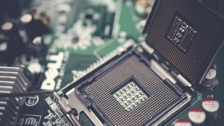
Wafer Level Packaging (WLP for short) is an advanced packaging technology, which has developed rapidly in recent years due to its advantages of small size, excellent electrical performance, good heat dissipation, and low cost. According to Verified Market Research, the wafer-level packaging market was valued at $4.84 billion in 2020 and is expected to reach $22.83 billion by 2028, growing at a CAGR of 21.4% from 2021 to 2028.
1. Wafer-level packaging VS traditional packaging
In traditional wafer packaging, the finished wafer is diced into individual chips, which are then bonded and packaged. Unlike traditional packaging processes, wafer-level packaging encapsulates the chip while it is still on the wafer. The protective layer can be adhered to the top or bottom of the wafer, then the circuit is connected, and the wafer is cut into individual pieces. chip.
Compared with traditional packaging, wafer-level packaging has the following advantages:
1. Small package size
Because there are no wires, bonding and plastic processes, the package does not need to expand out of the chip, making the package size of WLP almost equal to the chip size.
2. High transmission speed
Compared with traditional metal lead products, WLP generally has shorter connection lines, and will perform better under high performance requirements such as high frequency.
3. High-density connection
WLP can use an array connection, the connection between the chip and the circuit board is not limited to the periphery of the chip, and the connection density per unit area is improved.
4. Short production cycle
In the whole process of WLP from chip manufacturing to packaging to finished products, the intermediate links are greatly reduced, the production efficiency is high, and the cycle is much shortened.
5. Low process cost
WLP completes packaging and testing at the silicon wafer level, and achieves the goal of cost minimization by mass production. The cost of WLP depends on the number of qualified chips per wafer, and the trend toward smaller chip designs and larger wafer sizes has resulted in a corresponding reduction in the cost of a single device package. WLP can make full use of wafer fabrication equipment, and the cost of production facilities is low.
2. Process flow of wafer level packaging
The wafer level packaging process flow is shown in the figure:
1. Coat the first layer of polymer film to strengthen the passivation layer of the chip and play the role of stress buffer. The types of polymers include photosensitive polyimide (PI), benzocyclobutene (BCB), and polybenzoxazole (PBO).
2. The redistribution layer (RDL) is to rearrange the position of the aluminum/copper pads of the chip, so that the new pads meet the requirements for the minimum spacing of the solder balls, and the new pads are arranged in an array. The photoresist is used as a template for selective electroplating to plan the circuit pattern of the RDL, and finally the photoresist and the sputtering layer are removed by wet etching.
3. Coating the second layer of polymer film to flatten the wafer surface and protect the RDL layer. New pad locations are lithographically etched on the second polymer film.
4. The under-bump metal layer (UBM) is made by the same process as RDL.
5. Plant the ball. The solder paste and solder balls are accurately positioned through the mask, and the solder balls are placed on the UBM and placed in a reflow oven. The solder is melted by reflow to form a good infiltration combination with the UBM to achieve a good soldering effect.
3. Development Trend of Wafer Level Packaging
With the continuous upgrading of electronic products, emerging markets such as smartphones, 5G, and AI have put forward higher requirements for packaging technology, making packaging technology develop in the direction of highly integrated, three-dimensional, and ultra-fine pitch interconnection. Wafer-level packaging technology can reduce chip size, wiring length, solder ball spacing, etc., so it can improve the integration of integrated circuits, processor speed, etc., reduce power consumption, and improve reliability. Low-cost development requires demand.
Wafer-level packaging technology should continue to reduce costs, improve reliability, and expand applications in large ICs:
1. Reduce the process cost and shorten the process time by reducing the number of WLP layers, mainly for products with few I/O and small chip size.
2. Improve the performance and reliability of WLP through the application of new materials. Mainly for products with many I/O and large chip size.