All that You Need to Know About HDI Printed Circuit Board
OriginalSource: https://www.klusster.com/portfolios/pcbtogo/contents/141447?code=58d351d9-34e2-453e-9638-949d380f078c&share_content=true
Themuch-increased packing density is the most prevalent rationale for employingHDI technology. As a result, components and their landing surfaces have accessto the area created by more acceptable track constructions. Furthermore, theoverall area demand lowers, resulting in a lower board size and fewer layersrequired.
FPGAs andBGAs with a pitch of 1mm or less are frequently available. When tracks arerouted between the pins, HDI technology makes it simple to route and join. Hereare the things that you will need to know.
Countlessbenefits such as fast speed, compact size, and high frequency are linked withHDI PCBs. The main components are mobile computers, PCs, and mobile phones.Moreover, in various user end devices, e.g., MP3 players and gaming consoles,HDI PCBs are widely employed.
HDI PCBs usethe latest technologies to enhance the functionality of circuit boards via thesame or small area quantity. The evolution of board technology is driven by thenarrowness of components and semiconductor packages that provide superiorfeatures for inventive new goods like tactile screen tabs.
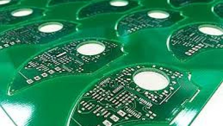
HDI-Printed Circuit Boards
A circuitboard has a diameter of 0.15mm (6 mils) to 0.1mm (4 mils) and can be drilledphysically or by laser (standard). The circuit board pad has a diameter of only0.3mm (12mil) due to a thin annular ring of only 0.1mm, which saves a lot ofspace compared to traditional Via pads.
Use of the Advanced Circuits
AdvancedCircuits is at the front of innovation, meeting the most stringent standardswith HDI PCB designs that push the boundaries of technology.
Because oftechnological breakthroughs and the numerous advantages, HDI PCBs provide forhigh-tech applications, demand for HDI PCB production has been growing.However, many PCB makers cannot fit more technology into less area with fewerlayers because they lack the specialized equipment and capacity for moredelicate lines, advanced features, as well as tighter tolerances. HDI PrintedCircuit Board designs combine sophisticated features such as circuit boards,via-in-pad, blind vias, stacked and staggered vias, and via-in-pad withstaggered and stacked vias to maximize board area while boosting performance aswell as functionality.
Perfect Competencies
Within-house laser drill competencies that include precise depth control, AdvancedCircuits achieves excellent quality and precision. In addition, all multilayer withinner cores is thoroughly inspected utilizing (AOI) Automated OpticalInspection units for exceptional fault identification of the most delicatedetails and direct laser imaging (LDI) capabilities for perfect registration.
Whenprototyping, there are many different types of PCBs to choose from, rangingfrom simple one-sided PCBs to more sophisticated multilayer boards. Copper tracks,or linkages between components on only one of the circuit board's surfaces, arethe most basic prototype printed circuit boards. Single-sided boards, or single-layer PCBs, are the name for these boards.
Conclusion
HDI PCBs, onthe other hand, are required in the production of increasingly complex boards. These printed circuit boards, alsoknown as High-Density Interconnect, contain a higher wiring density thanstandard PCBs. These boards have several advantages over traditional prototypecircuit boards, including narrower gaps, fewer vias, and a higher connectionpad density.