Global Wafer Bonding System Market
Global wafer bonding system market size was US$ XX Bn in 2019 and is expected to reach US$ XX Bn by 2027, at a CAGR of 10% during forecast period.
The report study has analyzed the revenue impact of COVID -19 pandemic on the sales revenue of market leaders, market followers, and market disrupters in the report, and the same is reflected in our analysis.
Market Definition
Wafer bonding is an advanced packaging technology or process in which two wafers of any materials are bond to each other at a room temperature. It is widely used for the fabrication of NEMS, MEMS, and microelectronics and optoelectronics devices.
Market Dynamics
A surge in the adoption of wafer bonding system in microelectronics industry to produce microelectronics devices is the major driving factor behind the growth of the market. Growing market for wafers with diameter of 200nm and 300nm, rapid growth in semiconductor manufacturing and electronics industry, ongoing development in various wafer bonding methods and growing market for advanced packaging and microfluidics technology are expected to improve the growth of market during the forecast period. The wafer bonding system provides some benefits such as low bonding temperatures, high compatibility with standard CMOS wafers and insensitivity to surface topography, which are ultimately propelling the growth of the market.
However, rising need for high voltage and temperatures and high costs of wafer fabrication process are the major restraining factor that could hamper the growth of the market.
Global Wafer Bonding System Market: Segmentation Analysis
By type, direct bonding segment dominated the market in 2019 and is projected to witness high growth at a CAGR of XX% during the forecast period. Direct bonding, a common type of wafer bonding process, does not require any extra intermediate layers. It is also called as fusion bonding process and it is based on the chemical bonds between two surfaces of any material. An increasing use of direct bonding process in applications such as in manufacturing of Silicon on insulator (SOI) wafers, actuators and sensors is accredited to the growth of the market.
The direct bonding process provides some benefits such as strong connection, increased compatibility, fast process, high bonding strength, high temperature stability and low cost, which is attracting various semiconductor manufacturing companies to adopt direct wafer bonding technology, which further results into growth of the market. In addition, increasing significance of direct wafer bonding process in fabrication of multi wafer micro structures such as micro pumps, micro valves, and accelerometers is expected to expand growth of the market in the coming years.
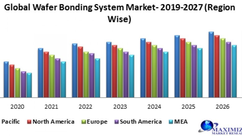
Global Wafer Bonding System Market: Regional Analysis
Region-wise, Asia Pacific held the largest market share in 2019 and is expected to maintain its dominance at a CAGR of XX% during the forecast period. The countries such as China, Japan, India, Taiwan, and South Korea are the major key contributors behind the growth of the market. The growth is attributed to the growing market for semiconductor manufacturing industry across the region.
The massive presence of various leading semiconductor manufacturing companies, increasing investments in the electronics manufacturing industries, growing market for electronic packaging industry and rising trend of smart connected devices and Internet of Things (IoT) based applications are driving growth of the market in APAC region.
The objective of the report is to present a comprehensive analysis of the Global Wafer Bonding System Market including all the stakeholders of the industry. The past and current status of the industry with forecasted market size and trends are presented in the report with the analysis of complicated data in simple language. The report covers all the aspects of the industry with a dedicated study of key players that includes market leaders, followers and new entrants. PORTER, SVOR, PESTEL analysis with the potential impact of micro-economic factors of the market has been presented in the report. External as well as internal factors that are supposed to affect the business positively or negatively have been analyzed, which will give a clear futuristic view of the industry to the decision-makers. The report also helps in understanding Global Wafer Bonding System Market dynamics, structure by analyzing the market segments and projects the Global Wafer Bonding System Market. Clear representation of competitive analysis of key players by Application, price, financial position, Product portfolio, growth strategies, and regional presence in the Global Wafer Bonding System Market make the report investor’s guide.
Scope of Global Wafer Bonding System Market
Global Wafer Bonding System Market, By Type
• Direct Bonding
• Anodic Bonding
• Solder/Eutectic/ Diffusion Bonding
• Glass-Frit Bonding
• Adhesive Bonding
• Others
Global Wafer Bonding System Market, By Application
• Semiconductor
• Solar Energy
• Opto-electronic
• MEMS
• Others
Global Wafer Bonding System Market, By Region
• North America
US
Canada
• Europe
UK
France
Germany
Italy
Spain
Norway
Russia
• Asia Pacific
China
India
Japan
South Korea
Australia
Malaysia
Indonesia
• South America
Brazil
Mexico
Argentina
• Middle East and Africa
Global Wafer Bonding System Market, Key Players
• 3M
• Applied Microengineering
• Ayumi Industry
• Dynatex International
• EV Group
• NxQ
• Palomar Technologies
• SüSS Microtec SE
• Tokyo Electron
• Micronit Microtechnologies
• Mitsubishi Heavy Industries Machine Tool Co., Ltd.
• Coral Foodstuff Machine Co., Ltd
• Komachine.com, Co
• Thermo Electric Company, Inc.
• Logitech LTD
• Electron-Mec s.r.l
• Inseto
• XX
• XX
For more information of visit:https://www.maximizemarketresearch.com/market-report/global-wafer-bonding-system-market/74075/
This report submitted by Maximize market Research Company
Customization of the report:
Maximize Market Research provides free personalized of reports as per your demand. This report can be personalized to meet your requirements. Get in touch with us and our sales team will guarantee provide you to get a report that suits your necessities.
About Maximize Market Research:
Maximize Market Research provides B2B and B2C research on 20,000 high growth emerging opportunities & technologies as well as threats to the companies across the Healthcare, Pharmaceuticals, Electronics & Communications, Internet of Things, Food and Beverages, Aerospace and Defense and other manufacturing sectors.
Contact info:
Name: Lumawant Godage
Organization Address: MAXIMIZE MARKET RESEARCH PVT. LTD.
Email: sales@maximizemarketresearch.com
: Omkar Heights,
Sinhagad Road,
Manik Baug,
Vadgaon Bk,Pune,
Maharashtra 411051,
India.
Contact: +919607195908